

Stock code:688130
- Application
 Smart Health Scale
 Medical Electronic
 Industrial control and meter
 Smart Sense
 - Products
Industrial Control Application ICMeasurement sensor ICMetrology ICDigital Temperature Sensor
- Services
- About Us
- News
Flash
120k
SRAM
8k
ADC ENOB
19.5bits@15.2sps
Gain=128
Gain=128
LCD
44SEG*4COM
Communication Port
2 UART,1 I²C,1 SPI
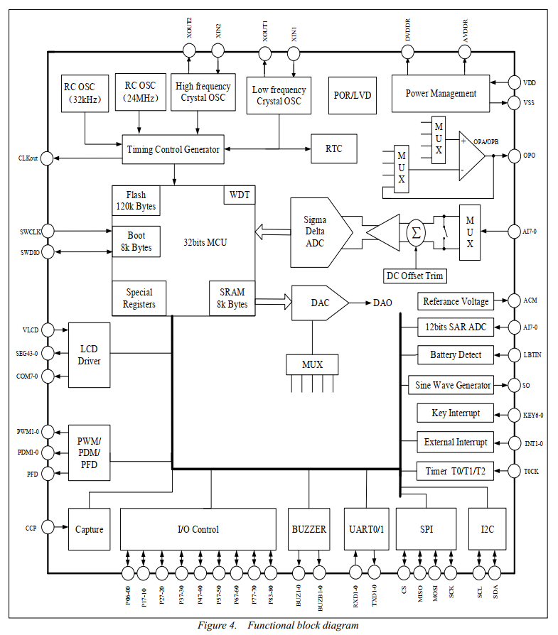
The SD93F115 is a 32 bits MCU CMOS SoC with built-in high precision 24 bits ADC, LCD driver, and 120k bytes flash program memory.
The 32bits system can be read by byte, half word (16 bits), and full word (32 bits). When the power is on the system clock is 12MHz by default. Different frequencies can be selected through register configuration. The maximum frequency is 24MHz.
Four working modes are provided so users can select the optimum choice between speed and power. The modes are: normal, standby (WAIT), sleep (DOZE), and deeply sleep (STOP).
High precision ADC, 18.6bits ENOB at 8sps (Gain = 256). It can be set to 4 differential or 8 single-ended inputs
Low noise, high input impedance preamplifier with offset calibration and selectable gain options: 1, 4, 8, 16, 32, 64, 128 or 256
12 bits SAR ADC with self-calibration function. Sampling rate and operation mode are selectable
32 bits MCU, 120k Bytes Flash, 8k Bytes Boot and 8k Bytes SRAM
Internal 24MHz and 32kHz RC oscillator with ±1% typical error after calibration
RTC module with external 32.768kHz crystal provides calendar/time information, including leap year. Timing accuracy is adjustable.
33SEG x 4COM, 32SEG x 5COM, 31SEG x 6COM, 29SEG x 8COM LCD drives with ultra-low power consumption and high driving capability. The IC has a programmable boost module to maintain luminance at low supply voltage. Drive voltage range: 2.7~5.2V
Built-in sensor excitation output. Voltage is 2.4~4.5V at 0.3V step
Built-in burnout detect current source
1.2V benchmark output
Built-in sine wave generator with selectable output frequency at 5kHz, 50kHz, 100kHz, and 200kHz. It supports an 8-electrode BIA fat measurement
Two operational amplifiers: OPA and OPB
Flexible low voltage detection and touch button detection circuits including an 8bits DAC and a rail-to-rail input comparator. The voltage detection range is 2.0~5.3V
Built-in silicon temperature sensor with single-point correction, automatic forward and reverse measurement
Peripheral resources include: UART, I2C, SPI, PWM/PDM, CCP, TIMER, Buzzer, 2 external interrupts, and 7 key interrupts
All I/O have Schmidt trigger inputs and pull-up resistors. The resistance of the pull-up resistor is 50kΩ
Operating voltage range: 2.4~5.5V
Operating temperature range: -40~85℃

-
 Download
-
 Sample Requests and Purchase
-
 Q&A
Q&A
-
 Online Support
Products
Hangzhou Headquarter
Tel:15325714186
Email:sales-2@drivrfchk.com
Address:5/F, Bldg4, Topsun Technology Park 351 Changhe Road, Binjiang District Hangzhou, Zhejiang, China
Postal Code:310052